
Solid-State and Lithium-Sulfur Batteries: The Next Breakthrough in Energy Storage?
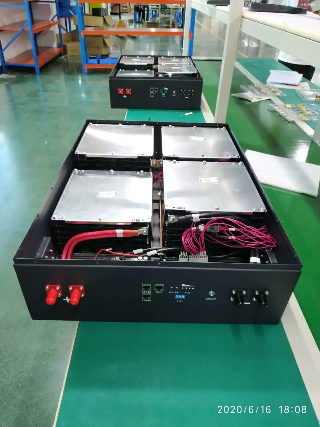
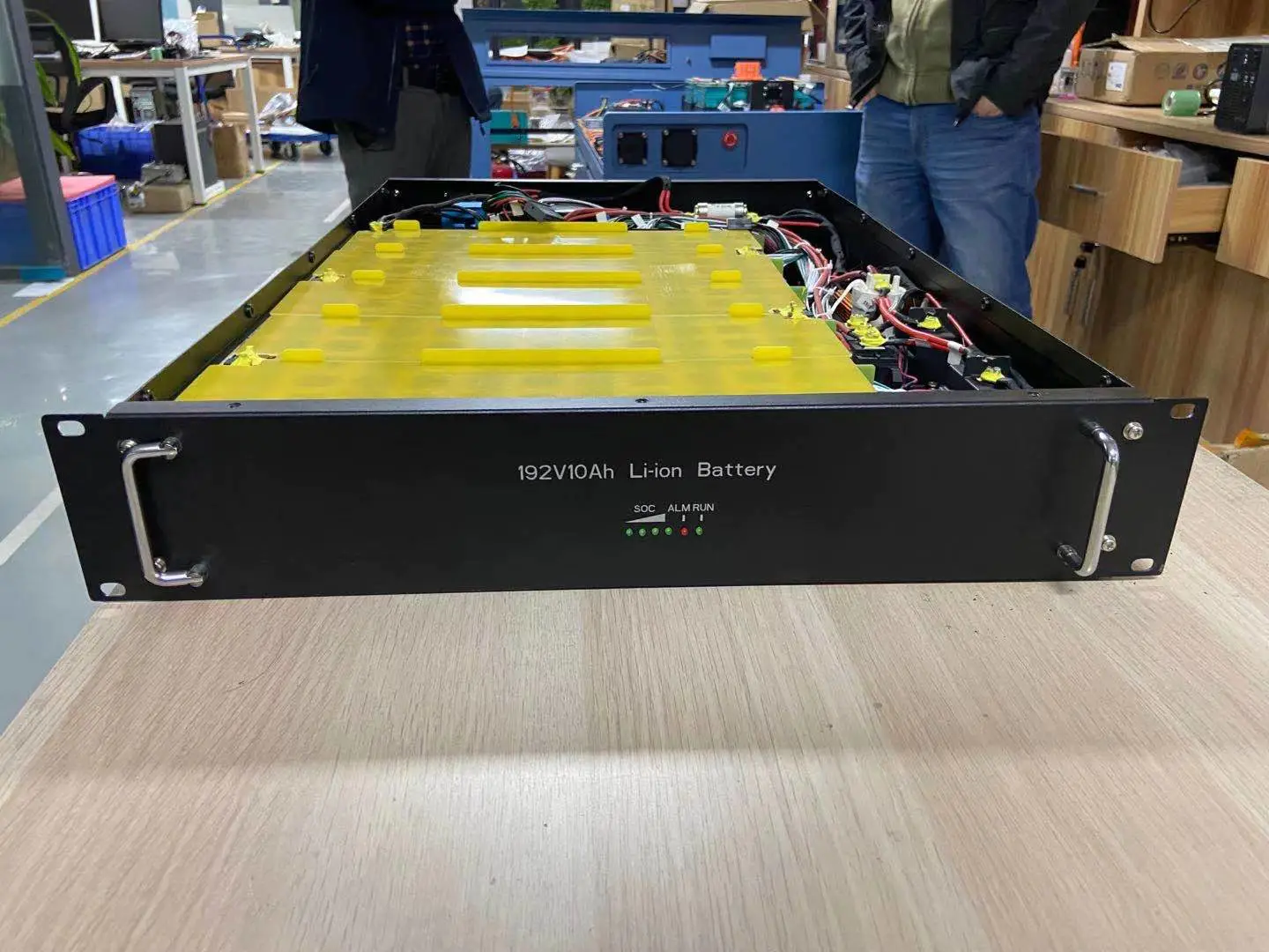
EV battery
How does buck-boost charging + USB Type-C™ PD improve power density?
by:Vglory
2021-03-30
In recent years, the buck-boost charger has become more and more popular because it can charge the battery from almost any input source, regardless of whether the input voltage is higher or lower than the battery voltage. One of the key advantages of USB Type-C being widely used is that it is considered to be the ideal plan for completing universal adapters and reducing the corresponding electronic waste reduction. Although the USB Type-C interface is the same, the rated power and voltage of different adapters are still very different. This includes traditional 5 V USB adapters and USB PD adapters that can supply voltages from 5 V to 20 V. In addition, the number of batteries in series in different portable devices may also be different. This requires the battery charger integrated circuit (IC) to choose a buck-boost topology to adapt to these arbitrary changes in input voltage and battery voltage. The buck-boost charging chip with high power density can not only integrate common charging function modules, but also other components in the USB PD charging system, such as load switches and DC/DC converters, to simplify system planning and reduce materials List (BOM) cost, and adhere to the overall solution plan of small size. Figure 1 shows the system block diagram of the USB PD charging solution plan. Figure 1 shows the support for mobile USB OTG charging standards. When the adapter does not exist, the battery is discharged through the DC/DC converter, and a stable voltage is output at VBUS to supply power to external devices. If the USB Type-C port needs to support the function of Fast Role Communication (FRS), it is necessary to open the DC/DC converter and always be in standby, even if the adapter has been pierced into the USB Type-C port. When the adapter is disconnected, the back-to-back MOSFETs in the discharge power path are quickly turned on, passing the U3 output voltage to VBUS and keeping the VBUS voltage from falling. In this process, always insisting that the DC/DC converter is open will actually form a rated static current loss for the entire system. The fully integrated buck-boost charging chip shown in Figure 2 can simplify the system-level planning of the USB PD charging solution plan. First, integrate the input current detection circuit into the chip. After the input current detected by the circuit, the charger supplies input current conditioning and input current overcurrent maintenance to prevent the adapter from overloading. Secondly, as part of the input over-voltage and over-current maintenance circuit, the control logic and drive circuit of the external back-to-back MOSFET are also integrated into the charger. These functions make it possible to eliminate the unit supporting input power path management and input current detection from the block diagram. After completing the two-way operation of the buck-boost converter of four FETs, the charging chip itself can support the OTG mode. When the adapter pierces the USB port, the charging chip works in a forward charging mode, and power flows from VBUS to the battery. When the adapter is disconnected, power flows from the battery to VBUS. The OTG output voltage at VBUS covers the full USB PD voltage scale from 2.8 V to 22 V, has a programmable step length of 10mV, and is compatible with the USB PD 3.0 standard. Figure 2 In order to support the FRS function of the USB Type-C port, this integrated buck-boost charging chip has completed a new backup form. In this article, the standby mode refers to the rapid conversion of the buck-boost charging chip from the forward charging mode to the reverse OTG mode, so as to prevent the bus voltage from falling. Looking at the application block diagram in Figure 3, the adapter is connected to the USB port to power the system and charge the battery through a buck-boost power stage. At the same time, the adapter can supply power to the system accessories from the PMID output of the charger. If the buck-boost charging chip does not support the standby mode, when the adapter is disconnected and removed, the battery can still supply power to the system through the FET inside the chip. However, the accessory power supply on the PMID may lose power. After the charging chip is enabled in the standby mode, the VBUS voltage can be monitored. The voltage drop of VBUS below the preset threshold can be used as a signal that the adapter has been removed. Once the charging chip detects that the adapter has been removed, it will quickly switch from the forward charging mode to the reverse OTG mode, use the energy discharged from the battery to maintain the VBUS voltage, and complete FRS by itself. When the adapter is removed, the system itself and the power supply of the system accessories can be seamlessly switched from the adapter to the battery. This approach can eliminate the DC/DC converter for OTG and FRS from the block diagram. Figure 4 shows the test waveform of the alternate form of the charging chip used to support FRS. A 9 V adapter is connected to USB1 as the input power source. When the adapter is inserted, the charging chip turns on ACFET1-RBFET1 to connect the adapter to VBUS. The test condition of this waveform is that there is 1 A of current at PMID to supply power to the system accessories, and 1 A of charging current at BAT. When the 9 V adapter voltage (VAC) is removed, the charging chip quickly shifts from the forward charging mode to the reverse OTG mode, which can still maintain PMID and VBUS at 5 V, and together continue to supply power to the 1 A PMID load. All the functions described above in Figure 3 and Figure 4 help to simplify the system-level planning of the USB PD charging solution plan, and TI has completed the new buck-boost charging chips BQ25790 and BQ25792. These charging chips support the input voltage scale from 3.6 V to 24 V for charging 1 to 4 batteries in series, and the input scale covers the entire USB PD voltage scale. These functions choose 2.9 mm × 3.3 mm wafer size package or 4 mm × 4 mm square flat lead-free package. The entire charging solution plan can supply 45 W of power, and the power density is about 100 W/in2 (150mV/mm2), which is twice that of similar products in shopping malls. Disclaimer: The articles published on this site are all from the Internet and do not represent the views of this site. If there is any infringement, please contact to delete WeChat: Disclaimer: Some pictures and content of the articles published on this site are from the Internet. If there is any infringement, please contact delete A: What do you think of this electric bicycle with the power part designed by Ferrari?
Custom message
Related Products


![[Industry Solution] How does outdoor backup power supply cope with extreme climate? Practical analysis of lithium solar cells](https://img80003422.weyesimg.com/uploads/vglorylibattery.com/images/17502322689034.jpg?imageView2/2/w/1920/q/70/format/webp)